

(3D-NAND,DRAM)
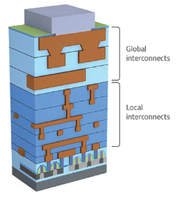
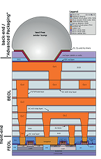
Packaging
WLP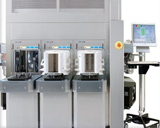
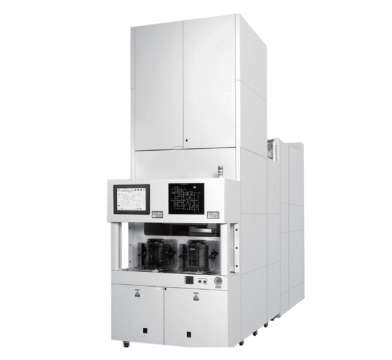
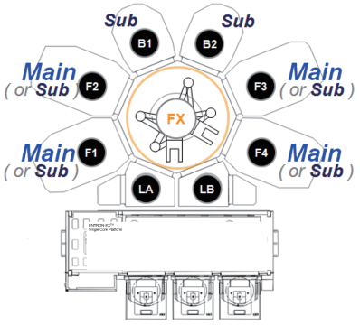
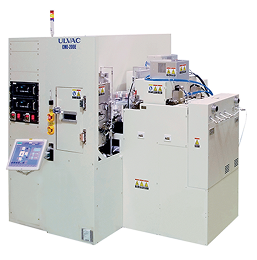
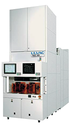
ENTRON™ EX300
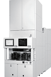
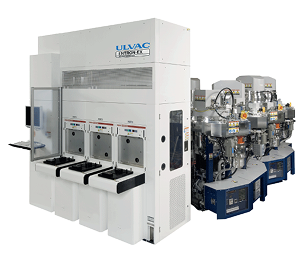
RISE™ 300


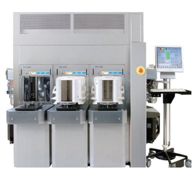

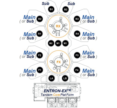
ENTRON™ SeriesDelivery Record > 500

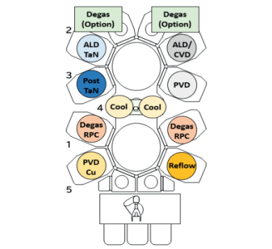
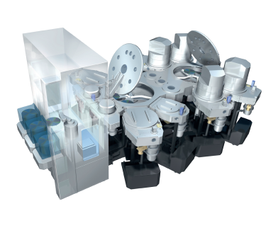
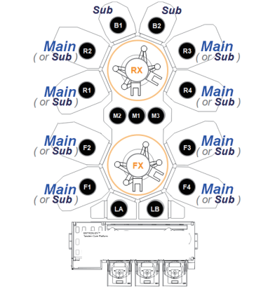
Main Process Module x 4 + Sub Process Module x 2 + Load Lock Module x 2
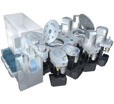

Main Process Module x 8 + Sub Process Module x 2 + Load Lock Module x 2

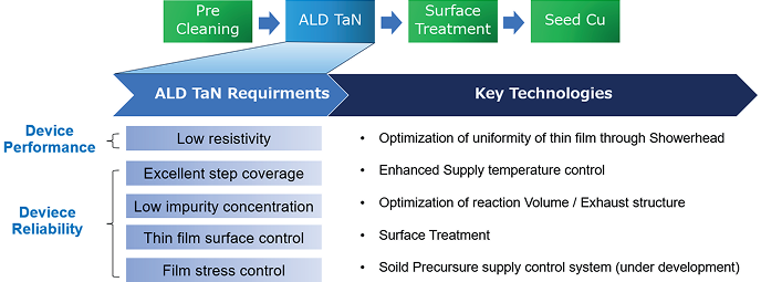
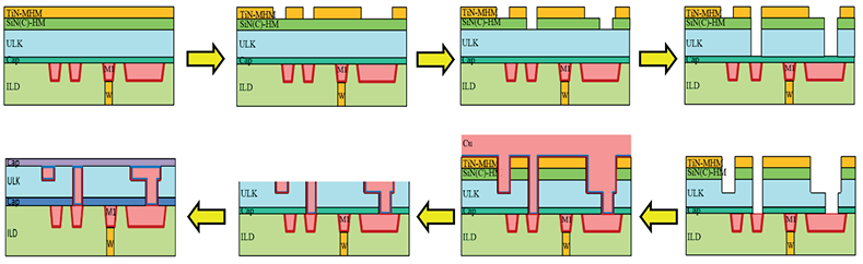
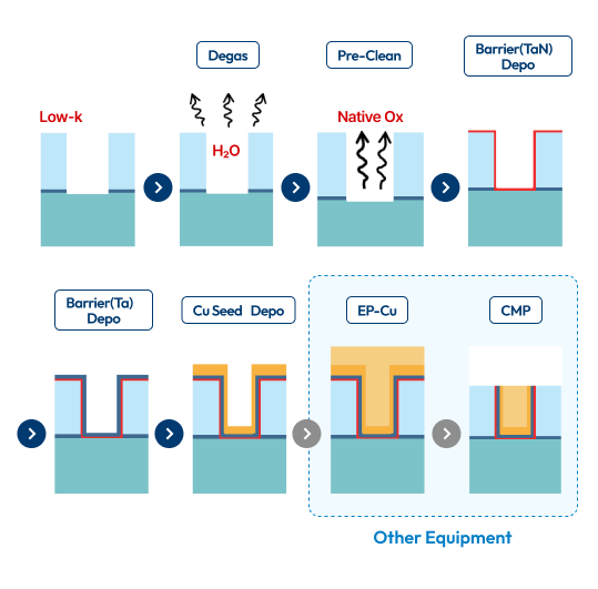
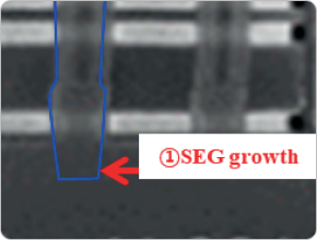
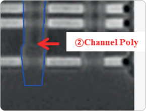
Cu Integraion Process Flow (In situ)
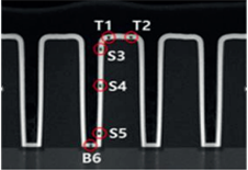
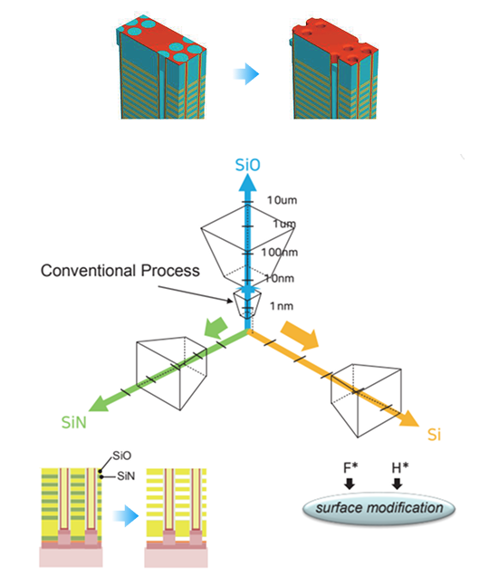
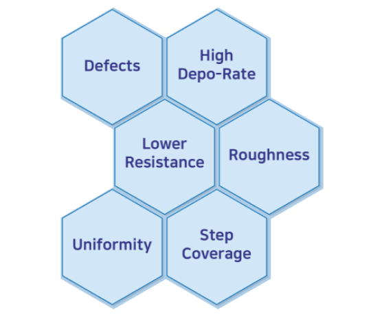
Excellent step coverage
in narrow patterns
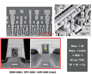
Logic Interconnect (Small,Fine Pitch)


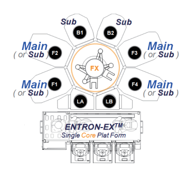
ENTRON™-EX W300 Single System
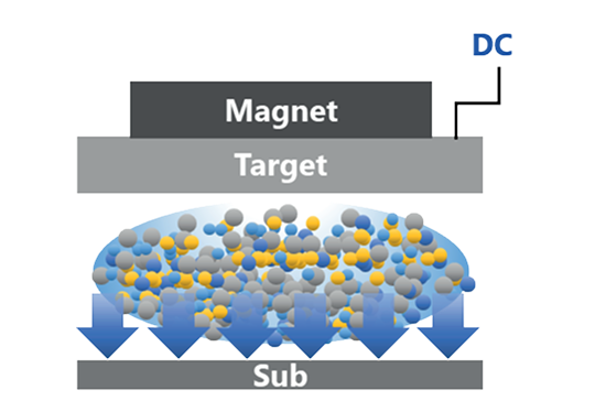
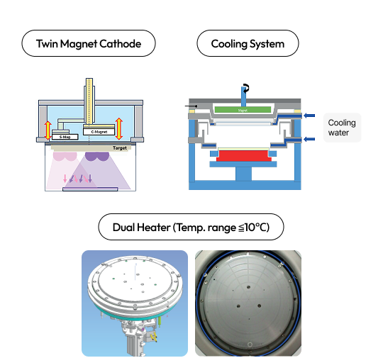
High plasma density High ionization

Tunable film stress for TiN films with high density Implementing high ionization with Conventional
PVD-based technology
ENTRON-EX W300 Tandem System
Cutting edge technology to Thin& thick films
High Throughput and performance with multi
cluster chamber
Crystallinity control, Thermal stability
Lower resistance, Higher reliability interconnection
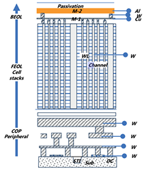
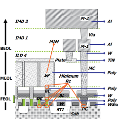
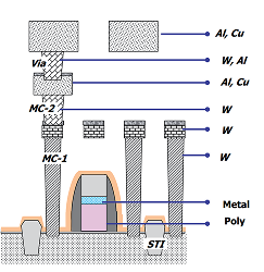
LOGIC
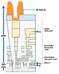
DRAM
NAND

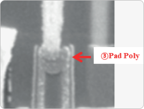
Cu / Ta / TaN@TEM Image
(ULVAC Pattern)
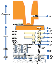
Logic
DRAM


Low resistivity can be achieved
by controlling nucleation
and process method in the sputtering process
Normal W
15% improvement
ULVAC Low
Resistivity W

in resistivity of W

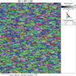
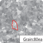
Grain Size & crystal orientation
increase by EBSD
Logic : Interconnection, DRAM & NAND : Gate Electrode, Interconnection, etc.
LOGIC
DRAM
NAND
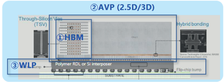
WLP for Cu-RDL : RDL with Chip middle structure, Up to 8 stacked
HBM for Seed layer : Seed layer for micro bump pad to access TSV
2.5D Packaging, Hybrid Bonding, …
| SFEM /Core |
|
|---|---|
| Degas |
|
| Pre-Clean |
|
| Sputter |
|
GPU structure
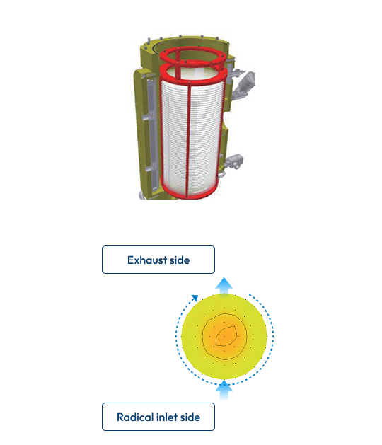
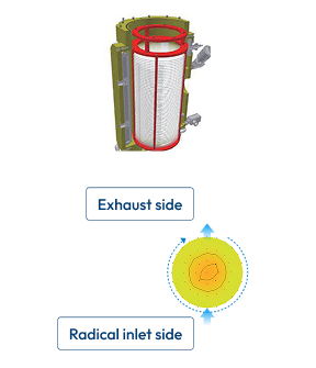
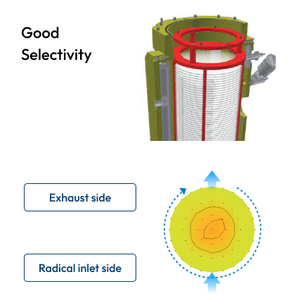
2 Microwave Applicator Plasma Damage
Free Source
2 Microwave Applicator Plasma Damage
Free Source
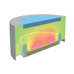
Wafer Surface Clean Roughness Excellent
CVD Module
PVD Module
Dry Clean Module
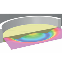
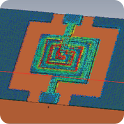
Target erosion profile
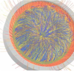
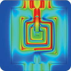
Plasma electron tracks
Deposition profile
on the substrate
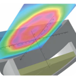
Voltage distribution
E-Field on plane
RF surface current
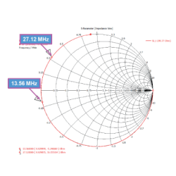
Smith chart(Matcher)
Voltage distribution
COPYRIGHT©2025 한국알박㈜ ALL RIGHTS RESERVED


